|
CMOS monolithic active pixel sensors for charged particle
tracking applications
|
 |
|
| |
|
C. Andreoli, M. Manghisoni, E. Pozzati, L. Ratti, V. Re,
V. Speziali, G. Traversi
|
|
|
Monolithic active pixel sensors (MAPS) in CMOS technology are
considered very promising as a replacement or a valid competitor with
CCD detectors in many applications. The main reason for the ever
growing interest in CMOS MAPS lies in the opportunity of integrating
analog and digital processing electronics together with the sensor
array in the same substrate, taking advantage of the large scale of
integration and low power dissipation available through commercial,
low-cost CMOS processes. In the last few years, many efforts were made
to extend the application field of CMOS MAPS to high-granularity
particle detection in high energy physics experiments. The interest of
the particle physics community for monolithic active pixel sensors
stems from them being a possible solution to the material budget issue
put forward by the experiments to be run at the future colliders.
|
|
|
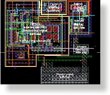
This research activity is concerned with the feasibility study of a
new implementation of CMOS monolithic active pixel sensors (MAPS) for
applications to charged particle tracking. As compared to standard
three MOSFET MAPS, where the charge signal is read out by a source
follower, the proposed front-end scheme relies upon a charge sensitive
amplifier (CSA), embedded in the elementary pixel cell, to perform
charge-to-voltage conversion. The area required for the integration of
the front-end electronics is mostly provided by the collecting
electrode, which consists of a deep n-type diffusion (deep n-well,
DNW), available as a shielding frame for n-channel devices in deep
submicron, triple well CMOS technologies. Based on the above concept,
a chip (called Apsel, active pixel sensor electronics), which includes
several test structures differing in the sensitive element area, has
been fabricated in a 0.13 um CMOS process. Tests with laser and
radioactive sources have demonstrated that the sensor is capable of
detecting ionizing radiation. The same design criteria have been used
in the development of a prototype monolithic CMOS sensor for the
vertex detector of one of the International Linear Collider (ILC)
experiments. In this prototype, the readout architecture takes
advantage of a sparsification technique to reduce the amount of data
to be sent off the chip, therefore complying with the time constraints
set for the ILC environment.
|
|